 precision positioning of EBID tip within few nanometers
precision positioning of an EBID tip on a W tungsten tip
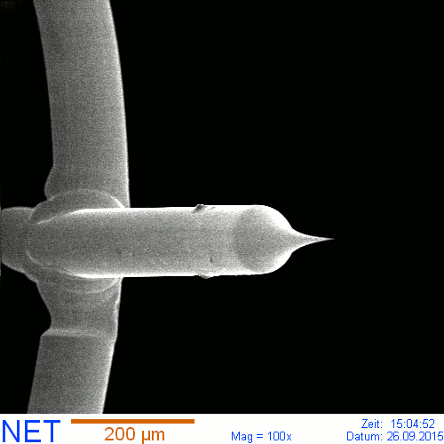 tungsten hairpin wire with etched tungsten needle tip, length of needle is 1 mm
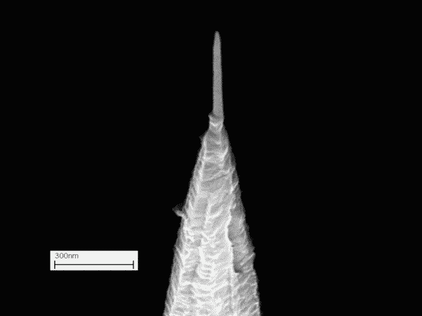
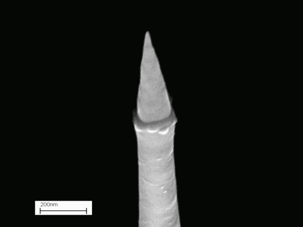
 tungsten needle tip with EBID cold field emitter supertip on tungsten shpere, length of supertip 1 µm
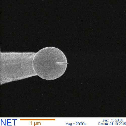
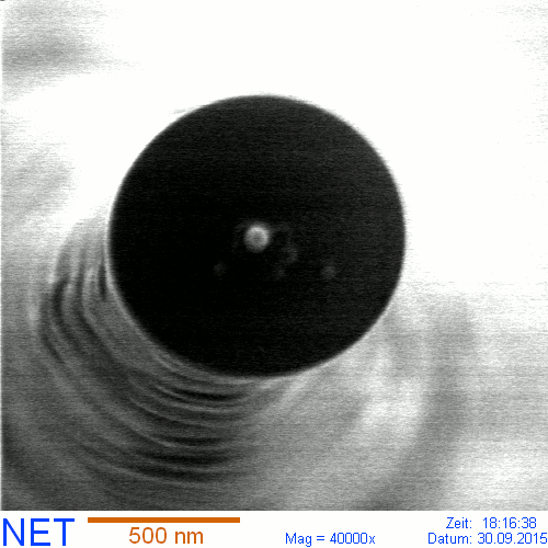 top view onto tungsten sphere with EBID supertip
standard tungsten hairpin wire with sharp tungsten needle having spherical end and EBID supertip for operation as cold electron field emitter, operating voltage is about 200 V.
left image: macroscopic view of tungsten needle
middle image: top of tungsten needle with EBID supertip, tilt angle 30 degree
right image: top view onto tungsten tip end with EBID supertip centered on tungsten sphere
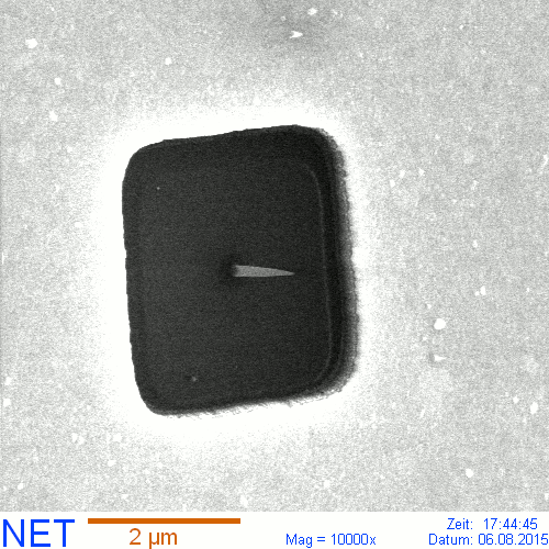 EBID emitter in MEMS extraction opening, tilted view
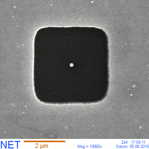 EBID emitter in MEMS extraction opening, top view
micrometer sized cold electron field emitter:
EBID emitter fabricated in MEMS extraction structure, operating voltage is about 100 V,
MEMS structure fabricated in-house by e-beam lithography.
left image: extraction aperture in MEMS device with EBID emitter tip in the center, tilted view
right image: top view of EBID emitter centered in MEMS device extraction aperture
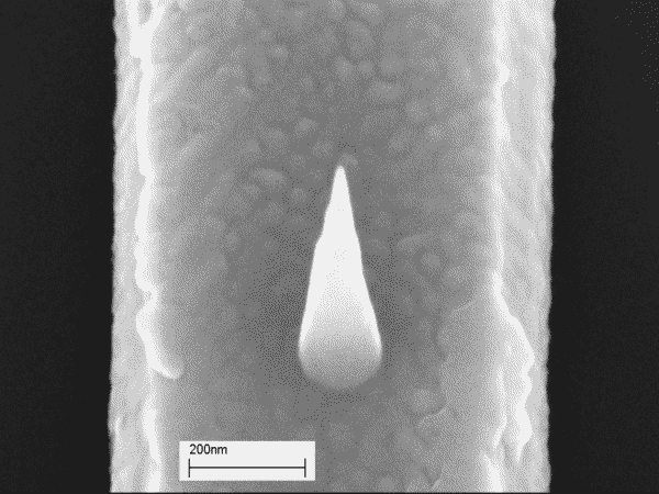
 cone shaped EBID tip geometry for enhanced mechanical stability
precision conical shaped EBID tip on etched W tip
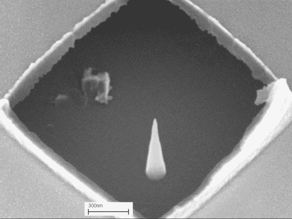 EBID tip in MEMS extraction structure
conical shaped EBID tip in an extraction opening produced by MEMS technology, MEMS structure provided by customer
 EBID tip on Au conduction line, building an electron emitter on an electrically insulation substrate
EBID tip in the center of a Au conduction line. Au conduction line is fabricated by e-beam lithography on a MEMS device.
![]()
nanoelectrotec - the combination of nanostructuration and vacuum electronics